- 您现在的位置:买卖IC网 > Sheet目录473 > MAX2510EVKIT-SO (Maxim Integrated)EVAL KIT MAX2510
�� �
�
�Low-Voltage� IF� Transceiver� with�
�Limiter/RSSI� and� Quadrature� Modulator�
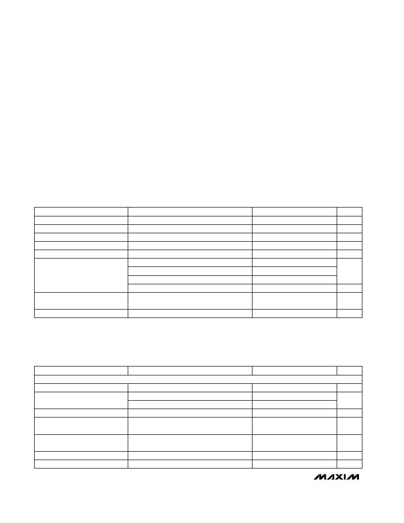
�ABSOLUTE� MAXIMUM� RATINGS�
�V� CC� to� GND� .............................................................-0.3V� to� 8.0V�
�V� CC� to� Any� Other� V� CC� ........................................................±0.3V�
�I,� I� ,� Q,� Q� to� GND� .........................................-0.3V� to� (V� CC� +� 0.3V)�
�I� to� I� ,� Q� to� Q� Differential� Voltage� ............................................±2V�
�RXIN� to� RXIN� Differential� Voltage� ..........................................±2V�
�LOIN� to� LOIN� Differential� Voltage..........................................±2V�
�LIMIN� Voltage� .............................(VREF� -� 1.3V)� to� (VREF� +� 1.3V)�
�RXEN,� TXEN,� GC� Voltage...........................-0.3V� to� (V� CC� +� 0.3V)�
�RXEN,� TXEN,� GC� Input� Current� ............................................1mA�
�RSSI� Voltage...............................................-0.3V� to� (V� CC� +� 0.3V)�
�Continuous� Power� Dissipation� (T� A� =� +70°C)�
�QSOP� (derate� 10mW/°C� above� +70°C)� ........................650mW�
�Operating� Temperature� Range� ...........................-40°C� to� +85°C�
�Junction� Temperature� ......................................................+150°C�
�Storage� Temperature� Range� .............................-65°C� to� +165°C�
�Lead� Temperature� (soldering,� 10sec)� .............................+300°C�
�Stresses� beyond� those� listed� under� “Absolute� Maximum� Ratings”� may� cause� permanent� damage� to� the� device.� These� are� stress� ratings� only,� and� functional�
�operation� of� the� device� at� these� or� any� other� conditions� beyond� those� indicated� in� the� operational� sections� of� the� specifications� is� not� implied.� Exposure� to�
�absolute� maximum� rating� conditions� for� extended� periods� may� affect� device� reliability.�
�DC� ELECTRICAL� CHARACTERISTICS�
�(V� CC� =� +2.7V� to� +5.5V;� 0.01μF� across� CZ� and� CZ� ;� LO,� LO� open;� MIXOUT� tied� to� VREF� through� a� 165� ?� resistor;� GC� =� 0.5V;� RXIN,�
�RXIN� open;� LIMIN� tied� through� 50� ?� to� VREF;� LIMOUT,� LIMOUT� =� open;� RXEN,� TXEN� =� high;� bias� voltage� at� I,� I� ,� Q,� Q� =� 1.4V;�
�T� A� =� -40°C� to� +85°C;� unless� otherwise� noted.� Typical� values� are� at� T� A� =� +25°C.)�
�PARAMETER�
�Operating� Voltage� Range�
�CONDITIONS�
�MIN�
�2.7�
�TYP�
�3.0�
�MAX�
�5.5�
�UNITS�
�V�
�Digital� Input� Voltage� High�
�Digital� Input� Voltage� Low�
�RXEN,� TXEN�
�RXEN,� TXEN�
�2.0�
�0.4�
�V�
�V�
�Digital� Input� Current� High�
�RXEN,� TXEN� =� 2.0V�
�6�
�30�
�μA�
�Digital� Input� Current� Low�
�RXEN,� TXEN� =� 0.4V�
�Receive� mode,� RXEN� =� high,� TXEN� =� low�
�-5�
�0.1�
�14�
�20�
�μA�
�Supply� Current�
�VREF� Voltage�
�Transmit� mode,� RXEN� =� low,� TXEN� =� high�
�Standby� mode,� RXEN� =� high,� TXEN� =� high�
�Shutdown� mode,� RXEN� =� low,� TXEN� =� low�
�V� CC� /� 2� -�
�100mV�
�17�
�0.5�
�0.2�
�V� CC� /� 2�
�25�
�1�
�5�
�V� CC� /� 2� +�
�100mV�
�mA�
�μA�
�V�
�GC� Input� Resistance�
�(Note� 1)�
�50�
�85�
�k� ?�
�AC� ELECTRICAL� CHARACTERISTICS�
�(MAX2510� test� fixture;� V� CC� =� +3.0V;� RXEN� =� TXEN� =� low;� 0.01μF� across� CZ� and� CZ� ;� MIXOUT� tied� to� VREF� through� 165� ?� resistor;�
�TXOUT� and� TXOUT� loaded� with� 100� ?� differential;� LO� terminated� with� 50� ?� ,� LO� AC� grounded;� GC� open;� LIMOUT,� LIMOUT� are� AC�
�coupled� to� 250� ?� load;� 330pF� at� RSSI� pin;� 0.1μF� connected� from� VREF� pin� to� GND;� P� RXIN,� RXIN� =� -30dBm� differentially� driven� (input�
�matched);� f� RXIN,� RXIN� =� 240MHz;� bias� voltage� at� I,� I� ,� Q,� Q� =� 1.4V;� V� I,Q� =� 500mVp-p;� f� I,Q� =� 200kHz;� f� LO,� LO� =� 230MHz;� P� LO� =� -13dBm;�
�T� A� =� +25°C;� unless� otherwise� noted.)�
�PARAMETER�
�CONDITIONS�
�MIN�
�TYP�
�MAX�
�UNITS�
�DOWNCONVERTER� (RXEN = high)�
�Input� Frequency� Range�
�(Note� 2)�
�100�
�600�
�MHz�
�Conversion� Gain�
�Noise� Figure�
�Input� 1dB� Compression� Point�
�Input� Third-Order� Intercept�
�T� A� =� +25°C�
�T� A� =� -40°C� to� +85°C� (Note� 3)�
�Single� sideband�
�(Note� 4)�
�Two� tones� at� 240MHz� and� 240.2MHz,�
�-30dBm� per� tone�
�20.5�
�19.9�
�22.5�
�11�
�-18.5�
�-8�
�25�
�25.5�
�dB�
�dB�
�dBm�
�dBm�
�LO� to� RXIN� Isolation�
�49�
�dBc�
�Power-Up� Time�
�Standby� to� RX� or� TX� (Note� 5)�
�5�
�μs�
�2�
�_______________________________________________________________________________________�
�发布紧急采购,3分钟左右您将得到回复。
相关PDF资料
MAX2511EVKIT
EVAL KIT MAX2511
MAX2538ETI+T
IC LNA/MIXER CELL/PCS/GPS 28TQFN
MAX2608EVKIT
EVAL KIT
MAX2611EUS+T
IC AMP LOW NOISE SOT143-4
MAX2616EVKIT#
EVAL KIT MAX2616
MAX2620EVKIT
EVAL KIT MAX2620
MAX2623EVKIT
EVAL KIT
MAX2632EUK+T
IC AMP 3V VHF/MICROWAVE SOT23-5
相关代理商/技术参数
MAX2511EEI
功能描述:射频收发器 IF Txr w/Limitr RSSI RoHS:否 制造商:Atmel 频率范围:2322 MHz to 2527 MHz 最大数据速率:2000 Kbps 调制格式:OQPSK 输出功率:4 dBm 类型: 工作电源电压:1.8 V to 3.6 V 最大工作温度:+ 85 C 接口类型:SPI 封装 / 箱体:QFN-32 封装:Tray
MAX2511EEI+
功能描述:射频收发器 IF Txr w/Limitr RSSI RoHS:否 制造商:Atmel 频率范围:2322 MHz to 2527 MHz 最大数据速率:2000 Kbps 调制格式:OQPSK 输出功率:4 dBm 类型: 工作电源电压:1.8 V to 3.6 V 最大工作温度:+ 85 C 接口类型:SPI 封装 / 箱体:QFN-32 封装:Tray
MAX2511EEI+T
功能描述:射频收发器 IF Txr w/Limitr RSSI RoHS:否 制造商:Atmel 频率范围:2322 MHz to 2527 MHz 最大数据速率:2000 Kbps 调制格式:OQPSK 输出功率:4 dBm 类型: 工作电源电压:1.8 V to 3.6 V 最大工作温度:+ 85 C 接口类型:SPI 封装 / 箱体:QFN-32 封装:Tray
MAX2511EEI-T
功能描述:射频收发器 IF Txr w/Limitr RSSI RoHS:否 制造商:Atmel 频率范围:2322 MHz to 2527 MHz 最大数据速率:2000 Kbps 调制格式:OQPSK 输出功率:4 dBm 类型: 工作电源电压:1.8 V to 3.6 V 最大工作温度:+ 85 C 接口类型:SPI 封装 / 箱体:QFN-32 封装:Tray
MAX2511EVKIT
功能描述:射频开发工具 MAX2511 Eval Kit RoHS:否 制造商:Taiyo Yuden 产品:Wireless Modules 类型:Wireless Audio 工具用于评估:WYSAAVDX7 频率: 工作电源电压:3.4 V to 5.5 V
MAX2514AWLX#G42
制造商:Maxim Integrated Products 功能描述:
MAX2514ELX
功能描述:射频发射器
RoHS:否 制造商:Micrel 类型:ASK Transmitter 封装 / 箱体:SOT-23-6 工作频率:300 MHz to 450 MHz 封装:Reel
MAX2514ELX-T
功能描述:射频发射器
RoHS:否 制造商:Micrel 类型:ASK Transmitter 封装 / 箱体:SOT-23-6 工作频率:300 MHz to 450 MHz 封装:Reel